01

Pcb design & layout
Production-ready PCB development from component placement and routing through design-rule verification, documentation, and fabrication release.

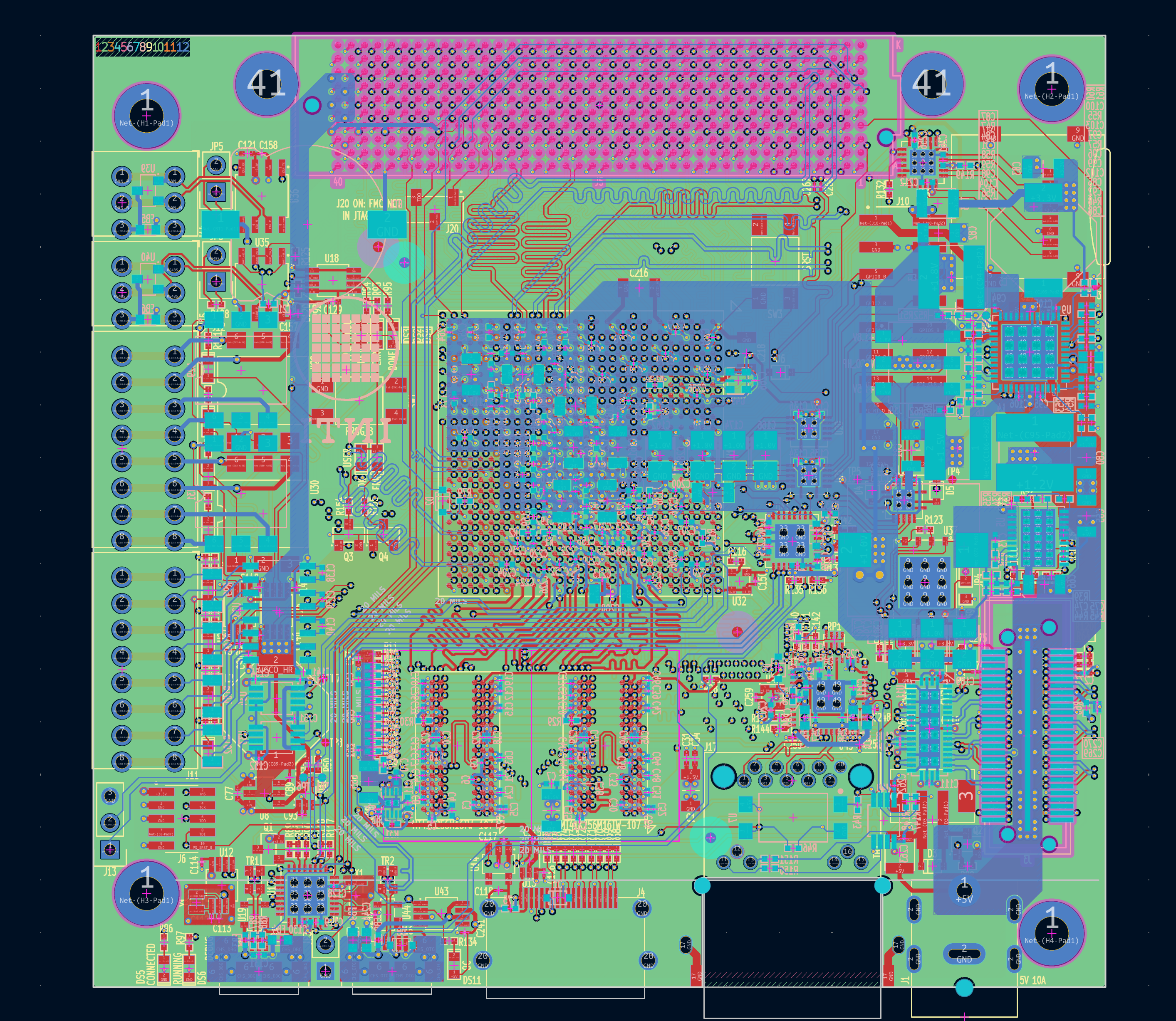
We provide the engineering expertise and capacity to develop complex PCBs, from architecture and stackup definition through layout, validation, and fabrication, while considering signal integrity, power integrity, EMC, and manufacturability from the beginning.
Production-ready PCB development from component placement and routing through design-rule verification, documentation, and fabrication release.
Design support for high-speed interfaces, controlled-impedance routing, differential pairs, signal integrity, and complex multilayer boards.
Power distribution, grounding, decoupling, and low-inductance layout strategies to support stable power delivery and minimize switching noise.
EMI-conscious PCB architecture, return-path management, grounding, filtering, and layout practices designed to reduce unwanted emissions and susceptibility.
Thermal-aware PCB design addressing component placement, copper distribution, thermal vias, heat dissipation, and operating reliability.
PCB designs optimized for fabrication and assembly, including stackup definition, DFM/DFT considerations, component placement, and manufacturing documentation.
Our process brings electrical, mechanical, and manufacturing considerations together from the earliest stages of PCB development. We define the board architecture and stackup, establish placement and routing requirements, and develop the design with performance, reliability, and manufacturing objectives in mind.
Deliver high-performance, reliable, and manufacturable PCB solutions that meet your product requirements from concept to production.